NiGK hopes this information could be any help for your business.
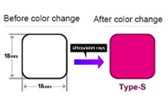
UV irradiation management by UV Label
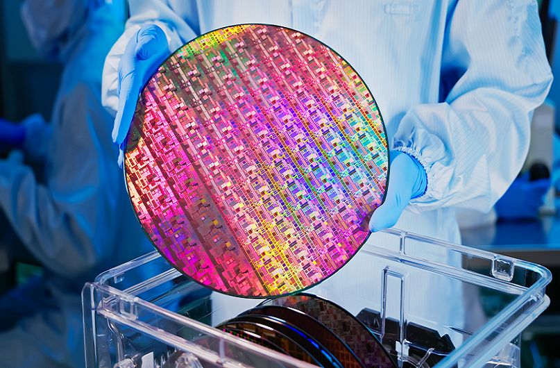
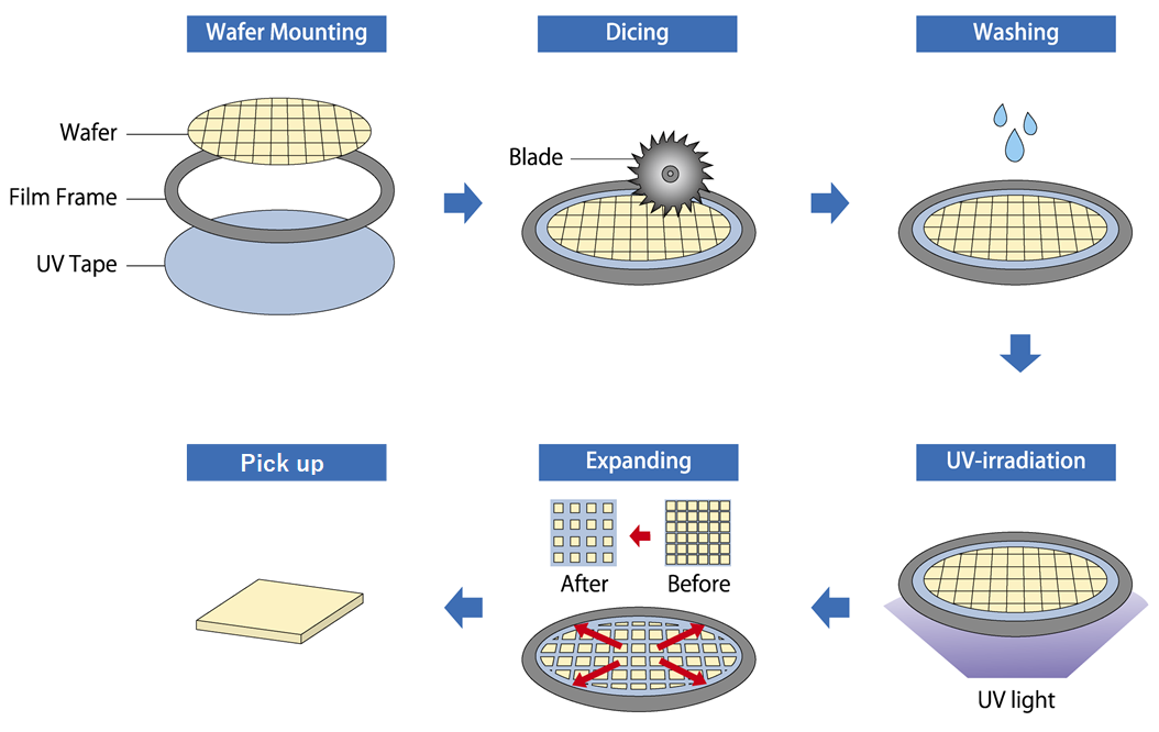
Dicing process
Before dicing (the process to separate dies from silicon wafer) , silicon wafers are typically mounted on dicing tape which the adhesive bond is broken by UV exposure.
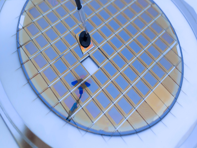
UV labels can check if the UV light is working correctly.
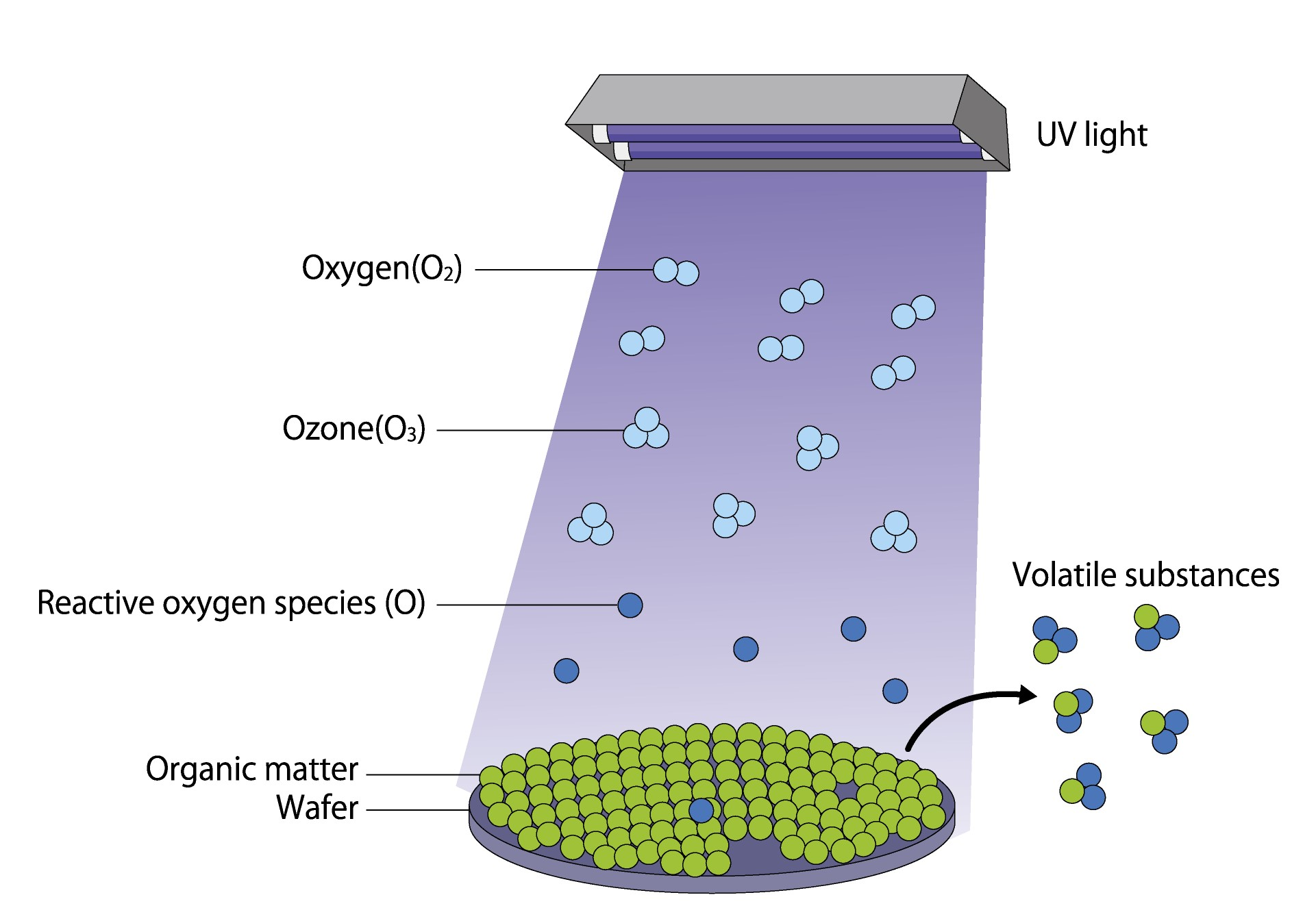
UV-Ozone cleaning process
UV irradiation generates ozone, which removes organic matter from the wafer surface.
UV labels can be used to check if UV-Ozone Cleaners are working correctly.
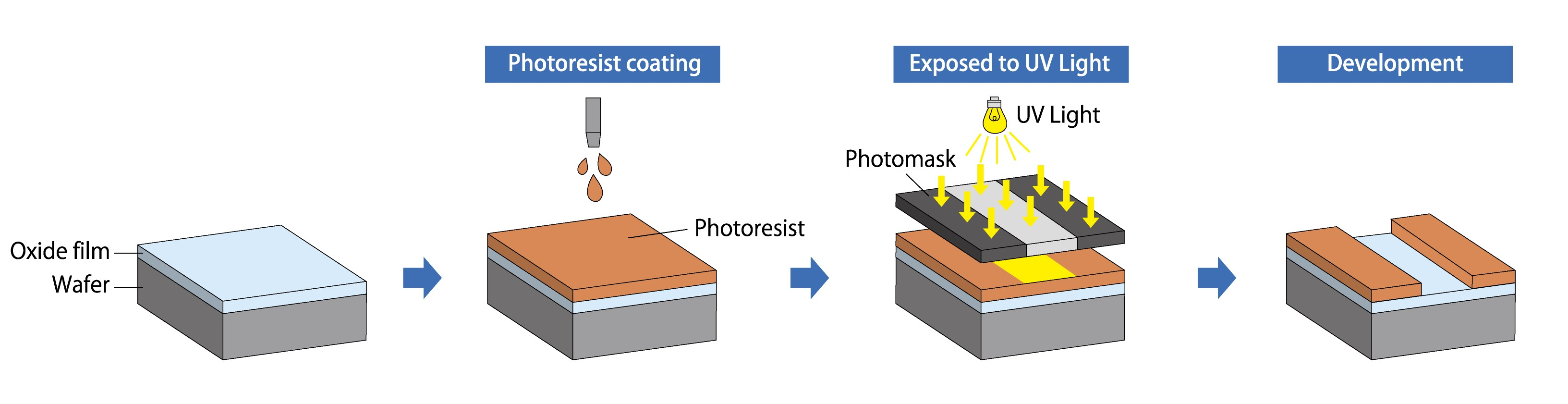
Photoresist Removal
Photoresist Removal is a process that removes photoresist from a silicon wafer. Photoresist melts when exposed to light and this makes it possible to create prominences and depressions. This allows for certain patterns to be created.
UV labels provide a solution for checking the irradiation distribution and intensity of the UV irradiation light source for Photoresist Removal.
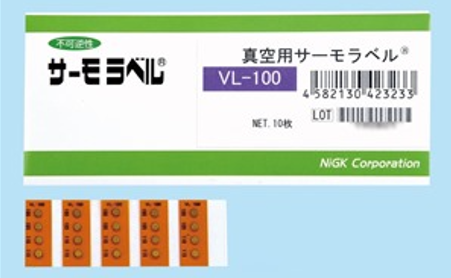
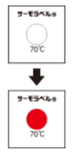
Temperature management by Temperature Label
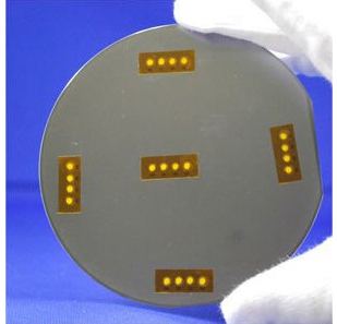
VL series can check temperature under vacuum
Vacuum condition makes easy to control chemical reactions and helps keeping the manufacturing space clean. If you attach the temperature indicators for vacuums (VL series) on a wafer, you can check the temperature easily even under the vacuum condition.
You can use temperature indicators in exhaust emission control system
Many kinds of chemical gases are used and emitted during the manufacturing process of semiconductors.
Temperature labels also can be used in a fan motor of an exhaust emission control system to check abnormal heat.
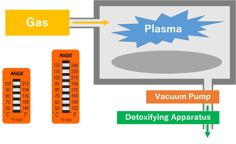
An image of exhaust emission control system
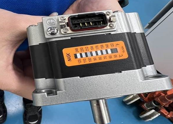
A part of motor of exhaust emission control system
For checking temperature in Chemical-mechanical polishing (CMP) process
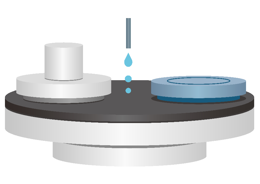
Chemical-mechanical polishing (CMP) process